domingo, 27 de junio de 2010

CRISTALOGRAFIA

COORDINACION

Coordinación
Se entiende por número de coordinación el número de vecinos inmediatos de un átomo, y por poliedro de coordinación, el poliedro resultante de la unión de los centros de los átomos de coordinación. Así, si un átomo está rodeado de tres átomos vecinos formando un triangulo plano, el número de coordinación és tres, y el poliedro (en este caso plano) un triangulo.


La coordinación en una estructura en que las partículas estructurales (las que se enlazan para formar la estructura cristalina) son átomos, depende de si el enlace es direccional o no.


En el caso de los enlaces direccionales (covalente), el número de vecinos de un átomo depende del número de orbitales de enlace, y el poliedro de coordinación, de las direcciones de estos orbitales. Por el contrario, en los casos de los enlaces no direccionales (metálico e iónico), como que la estructura más estable es la más compacta, el número y el poliedro de coordinación depende de los tamaños relativos de los átomos de la estructura: cada catión se rodea de tantos aniones como sea posible en función de sus tamaños relativos.

A continuación se hace un análisis de los posibles casos de coordinación en los enlaces NO direccionales:

a) si la diferencia de tamaños es muy grande, alrededor de un catión no hay lugar para tres aniones, y por tanto, solo habrá dos. En este caso la coordinación es lineal, y el número de coordinación dos.
En la figura se muestra este caso en una diagrama esquemático:

La estructura estable es de coordinación lineal porqué si fuese una coordinación mayor, por ejemplo 3, el átomo central "bailaría" en el espacio intersticial entre los aniones y la entropía de la disposición estructural a lo mejor sería demasiado grande.

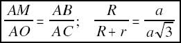
b) para que el catión tenga coordinación 3, debe ser tangente simultáneamente a los tres aniones, como se muestra en la siguiente figura


En el esquema de la derecha se puede comprobar que se cumple:


donde R y r son los radios del anión y del catión, respectivamente.
De aquí se deduce que r = 0.155R .
Esta relación es el límite inferior para que tenga lugar la coordinación triangular. Por debajo de este tamaño relativo habrá coordinación lineal, y por encima triangular, por bien que con tamaños ligeramente superiores, los tres
aniones no serán tangentes entre ellos, y solo lo serán con el catión.


c) Si el catión es mayor, puede llegar a un tamaño tal que quepan cuatro aniones a su alrededor, y por tanto se alcanza la coordinación cuatro. En estas
circunstancias, la disposición que tendría lugar es aquella que mantenga los aniones lo más separados posible para que se minimice la repulsión electrostática entre ellos: esta forma es un tetraedro, de manera que los centros de los aniones ocupan el vértice de un tetraedro, en el centro del cual está el catión.


Si se hace una sección para un de los planos diagonales del cubo de la figura de la izquierda, se obtiene el esquema de la derecha, en el cual


de donde se deduce que , que representa el límite inferior para r = 0.225R la coordinación tetraédrica, y por tanto se puede afirmar que entre las relaciones 0.155R y 0.225 R existirá coordinación triangular, mientras que por encima de 0.225R la coordinación será tetraédrica.

d) Para cationes de tamaños relativos respecto de los aniones más grandes puede llegar a darse coordinación octaédrica, es decir seis aniones alrededor del catión, los centros de los cuales dibujan un octaedro de coordinación alrededor del catión central. Haciendo una sección que pase por el centro de este octaedro queda un esquema como el de la figura siguiente:


En la cual:


donde a es la resta del octaedro, y de donde se deduce r = 0,414R que es el límite inferior para la coordinación octaédrica, de manera que entre esta relación y la anteriormente determinada habrá coordinación tetraédrica.

e) La siguiente coordinación posible es cúbica, con número de coordinación 8, como se muestra en la figura, una sección diagonal la cual permite establecer la relación de tamaños de radios necesaria para que se dé esta coordinación En la figura de la derecha se puede deducir:


y de aquí r = 0.732R que, como en los otros casos, es el límite inferior para la
coordinación cúbica.

f) Si los tamaños de los átomos son iguales, la coordinación que se da es 12, con un poliedro de coordinación, la forma del cual se puede ver en la siguiente figura, en que los átomos que rodean el central ocupan las posiciones de los centros de las aristas de un cubo:
Y considerando uno de los triángulos en que se divide el hexágono dibujado en la figura con líneas marrones:


Y como que sin30º=0.5, hay que concluir que r=R


Es decir que para que se de coordinación 12 hace falta que todas las esferas a empaquetar sean de la misma medida.

CRISTALOGRAFIA

FUERZAS DE ENLACE

Los átomos tienen cierta tendencia a unirse con otros átomos. La experiencia diaria de
observación de compuestos químicos de toda clase así lo sugiere, por tanto, imaginando un sistema muy simple formado por dos átomos aislados, es posible suponer que la interacción entre los dos es inversamente proporcional a la distancia d que los separa. La energía de atracción del sistema es
donde A es una constante que depende del tipo de átomos y m una que depende del tipo de enlace. Por tanto, la fuerza con que se atraen es la derivada de esta expresión:
Pero si solo existiese esta fuerza, que es más grande para distancias pequeñas, el sistema llegaría a colapsar porqué los dos átomos acabarían interpenetrados, y la experiencia demuestra que no es así, que los átomos tienen cierto tamaño y que los sistemas no colapsan. Debe existir, por tanto, una energía de repulsión que, a cierta distancia, contrarreste la de atracción. Por tanto, la energía del sistema debe ser

y de la misma forma, la fuerza total se obtiene derivando las dos energías:

respecto de las constantes m y n, dependiendo de la clase de atracción y repulsión que tenga lugar, se pueden considerar tres posibilidades m>n, m=n, y mSi m>n, la fuerza repulsiva es mayor a cualquier distancia, y por tanto los átomos no estarían unidos.

Si m=n, las dos fuerzas son iguales a cualquier distancia, y como antes, los átomos no estarían unidos.

Hay que admitir que m
distancias que la repulsión, y que esta no actúa significativamente hasta distancias muy pequeñas (cuando los átomos están muy cerca los núcleos también lo están y entonces actúa la repulsión electrostática). Si las dos anteriores expresiones se dibujan sobre un gráfico, dando valores arbitrarios a las constantes, queda un esquema como el de la figura siguiente


En la figura que muestra la gráfica de la energía hay un mínimo de la curva ET, que será la
energía de estabilidad del sistema (la mínima posible, de acuerdo con las previsiones de la Termodinámica) a 0ºK, en que los átomos estarán estabilizados a una distancia do. La derivada de un mínimo vale cero, por tanto, en la curva de la fuerza total la FT se anula para esta distancia do.
Sobre el sistema de los dos átomos no se ejerce ninguna clase de fuerza, y los átomos están quietos. Si se calienta el sistema (que equivale a suministrar energía), el sistema se sitúa en un nivel de energía E1. Para esta energía hay un intervalo de distancias (entre d'1 y d''1) para las cuales los dos átomos son estables. Si se observa la curva de fuerzas entre estas distancias se ve que para una distancia d'1d0 la fuerza entre los dos átomos es repulsiva. Lo que sucede es que los dos átomos están vibrando entre estas distancias.

Y si se calcula la distancia promedio entre ellos dos, como el pozo de la curva de ET es de
paredes asimétricas, se encuentra una distancia d1>d0: es decir, calentando el sistema se dilata.
Si se aumenta la energía del sistema a E2, las distancias a las que el sistema es estable están más separadas (los átomos vibran más, la vibración térmica aumenta), y su distancia promedio aumenta también.
Este esquema tan simple da una imagen dinámica del cristal más cercana a la realidad que la de un cristal estático, con los átomos estables (y quietos) en posiciones concretas. La realidad es que los átomos vibran alrededor de las posiciones de equilibrio, y existen unas fuerzas alternantes de repulsión y atracción que lo mantienen vibrando alrededor de una posición concreta.
Si se continua aumentando la energía del sistema, llega un momento en el que la fuerza de atracción que recupera el equilibrio entre los dos átomos no és suficiente, y el sistema ya no retorna al equilibrio. En términos de estructura, esta colapsa (el cristal funde) o se transforma en otra disposición estructural estable en las nuevas condiciones.


cristalografia

ESTRUCTURA CRISATALINA

LOS TAMAÑOS DE LOS ATOMOS Y DE LOS IONES
De hecho, en un átomo libre, la probabilidad radial de cualquier orbital mantiene valores positivos para distancias muy grandes, y desde este punto de vista, cada átomo tendría un radio infinito. Pero a nivel práctico, la posición de un electrón en un orbital se limita a la zona de mayor probabilidad radial. Por tanto, es posible hacer un cálculo de la zona de máxima probabilidad radial de cada átomo para tener una buena aproximación a sus medidas reales.Pero en una estructura cristalina los átomos no están libres, sino enlazados con otros, y además, hay cierta interpenetración de las capas electrónicas más externas, que participan del enlace. Por tanto, en una estructura cristalina se puede definir la distancia de enlace como aquella que separa los dos centros de dos átomos próximos.
En una aproximación un poco burda es posible admitir que la distancia del enlace es igual a la suma de los respectivos radios iónicos, de manera que:

d = r + r 1 2
Esta idea lleva necesariamente a admitir que el tamaño de los átomos será diferente de una estructura a otra, según sean los enlaces con los otros átomos y según cuales sean los átomos vecinos. De hecho, el tamaño de los átomos varia siguiendo dos factores:

a) el tipo y la polaridad del enlaceb) el número de átomos inmediatamente vecinos (el número de coordinación)

Existen algunas formulas empíricas que aproximan la distancia de enlace en función de los radios atómicos y de la diferencia de electronegatividades (que es una medida de la polaridad del enlace). Schomaker y Stevenson proponen la siguiente
d = r + r - - 1 2 1 2 0.09 c c
En las tablas que se pueden encontrar en muchos libros de Cristaloquímica, los radios iónicos están aproximadamente para una coordinación 6, y si el átomo entra en una estructura con otras coordinaciones hay que aplicar ciertas correcciones, como las que se muestran en la tabla siguiente, donde también se indican las correcciones para enlaces metálicos (el 100% corresponde a la coordinación 12, la más frecuente).

cristalografia

CRISTALOGRAFIA ESTRUCTURAL

Esta es la parte de la Cristalografía que estudia las estructuras cristalinas, es decir la disposición de los átomos y moléculas que forman el edificio cristalino, las causas de su ordenación, las propiedades que esta implica, etc.
De hecho, las propiedades de cualquier compuesto están controladas, no únicamente por su composición química, sino también por como sus átomos están distribuidos y enlazados en la estructura cristalina. Un caso paradigmático es el carbono, que en sus formas diamante y grafito da lugar a dos minerales de propiedades bien diferentes (entre ellas el precio).


En estos apuntes sobre Cristaloquímica se supone que el lector está familiarizado con la
estructura electrónica de los átomos, sus propiedades más significativas (potenciales de
ionización, electronegatividad...), así como con los tipos de enlace químico más comunes.


ENLACES QUIMICOS EN LOS CRISTALES


La manera como se ordenan los átomos en una estructura cristalina depende de las medidas de estos átomos y de las fuerzas de unión (de enlace) que mantienen las partículas estructurales juntas. Para una presión y temperatura determinadas, el conjunto de átomos de un cristal en equilibrio adopta una estructura que minimiza la entalpia libre G.


G = U + PV - TS


donde G es la entalpia de Gibbs, U la energía interna, P la presión, T la temperatura absoluta, V el volumen y S la entropía.


De acuerdo con esta expresión, a 0ºK la estructura más estable es la más compacta (que minimiza V) y la que tenga menor energía interna (U tiene signo negativo).
Por lo que hace referencia a la energía interna de un cristal (en valor absoluto) es la suma de las energías de enlace, las cuales a la vez, dependen de las fuerzas de atracción y repulsión de los átomos. La naturaleza de estas fuerzas determina el comportamiento físico-químico del cristal, y de hecho por eso, más adelante, se clasificarán de acuerdo con el tipo de enlace químico predominante.


En física se conocen tres tipos de fuerzas:
a) fuerzas gravitacionales, débiles y que operan a grandes distancias (astronómicas), vinculadas a la masa. Son las que mantienen en equilibrio el sistema planetario.
b) fuerzas eléctricas y magnéticas, mayores que las anteriores, ligadas a las cargas eléctricas y a sus desplazamientos, operan a distancias mucho menores que las gravitacionales.
c) fuerzas nucleares, aún más grandes, pero que operan a distancias muy pequeñas, prácticamente en el interior de los núcleos atómicos.


En una estructura cristalina, las fuerzas gravitacionales son despreciables, y si se considera el núcleo atómico una unidad indivisible, es posible considerar que en el interior del cristal operan las fuerzas eléctricas y magnéticas. No obstante, estas no se pueden estudiar con las leyes de la electrostática clásica (la ley de Coulomb, por ejemplo) porqué las cargas eléctricas (los electrones) están en movimiento y son demasiado pequeñas para que la mecánica newtoniana dé respuesta.. Su estudio requiere una aproximación a través de la mecánica cuántica.


No obstante se puede hacer una aproximación simple que permita explicar algunas de las estructuras cristalinas si se considera el núcleo atómico y las capas electrónicas saturadas como formando parte de un "interior" del átomo que no se modifica al formar parte de una estructura, y que los otros electrones (los de valencia) son los únicos que se reparten entre otros átomos para formar una molécula o una estructura cristalina.


Considerado de esta manera un cristal, la energía de este sistema se puede explicar con la electrostática clásica si se conocen las posiciones de los átomos y la repartición de la densidad
electrónica entre estos.

LA FORMA DE LOS ÁTOMOS Y DE LOS IONES


Una aproximación, suficiente para un primer nivel, a las estructuras de los cristales, es
considerarlas como un empaquetado de esferas de diferentes tamaños que representan los átomos y los iones que las forman. Esto equivale a imaginar los átomos de forma esférica, la cual cosa no se corresponde con las distribuciones de probabilidad radial de los orbitales que los forman: excepto los s, el resto tienen una forma más o menos lobular. En general se puede afirmar que la forma de un átomo será la suma de sus orbitales más exteriores ocupados

La forma de los metales alcalinos y alcalinotérreos (Li, Na, K, Rb, Fr, y Ca, Mg, etc.) Es esférica porqué lo es su orbital más externo (los 1s, 2s, 3s, 4s y 5s, respectivamente). Pero eso es diferente para los átomos que tienen ocupados orbitales p, como por ejemplo el boro (Z=5, configuración electrónica 1s2, 2s2, 2p1), que tendrá una forma claramente alargada. La situación es ligeramente diferente para el C (Z=6, que tiene semillenos los orbitales 2px y 2py) que tendría una forma de esfera aplanada, o para el N (Z=7) que con sus tres orbitales 2p semillenos, se parece más a la simetría esférica.

No obstante, en una estructura cristalina los átomos no están libres, sino enlazados con otros átomos. La tendencia de los átomos cuando se enlazan es acerca su configuración electrónica a la de un gas noble, la cual cosa suele estar más cercana a la forma esférica que el átomo libre. Los iones C+4 o el B+3 han perdido los electrones de los orbitales 2p y 2s, y su simetría esférica corresponde a la del nivel 1s.
El átomo libre de oxígeno (Z=8) tiene una configuración electrónica 1s2, 2s2, 2p4, mientras que el ión O-2 gana dos electrones respecto del átomo de oxígeno libre y como que tres orbitales 2p quedan saturados, adquiere una simetría más esférica. Igualmente pasa con el silicio (Z=14), las configuraciones electrónicas de su átomo libre y de su catión Si+4 son:
Si 1s2, 2s2, 2p6, 3s2, 3p2
Si+4 1s2, 2s2, 2p6
Es decir, que la aproximación a esferas de los átomos de las estructuras cristalinas, como un primer paso para su comprensión, no es descabellada, y se puede adoptar como modelo simple.

Cristalografia

CRISTALOGRAFIA

LA CRISTALOGRAFIA es la ciencia que se dedica al estudio y resolución de estructuras cristalinas. La mayoría de los minerales adoptan formas cristalinas cuando
se forman en condiciones favorables. La cristalografía es el estudio del crecimiento, la forma y la geometría de estos cristales.


La disposición de los átomos en un cristal puede conocerse por difracción de los rayos X. La química cristalográfica estudia la relación entre la composición
química, la disposición de los átomos y las fuerzas de enlace entre éstos. Esta relación determina las propiedades físicas y químicas de los minerales.

Cuando las condiciones son favorables, cada elemento o compuesto químico tiende a cristalizarse en una forma definida y característica.
Así, la sal tiende a formar cristales cúbicos, mientras que el granate, que a veces forma también cubos, se encuentra con más frecuencia en dodecaedros o
triaquisoctaedros. A pesar de sus diferentes formas de cristalización, la sal y el granate cristalizan siempre en la misma clase y sistema.

En teoría son posibles treinta y dos clases cristalinas, pero sólo una docena incluye prácticamente a todos los minerales comunes y algunas clases nunca se han observado.
Estas treinta y dos clases se agrupan en seis sistemas cristalinos, caracterizados por la longitud y posición de sus ejes. Los minerales de cada sistema comparten algunas
características de simetría y forma cristalina, así como muchas propiedades ópticas importantes.

METODOS
Los métodos cristalográficos se apoyan fuertemente en el análisis de los patrones de difracción que surgen de una muestra cristalina al irradiarla con un haz de rayos X,
neutrones o electrones. La estructura cristalina también puede ser estudiada por medio de microscopía electrónica.

Un material cristalino es aquel en el que los átomos se estructuran en redes basadas en la repetición tridimensional de sus componentes.
A la estructura que se repite se le denomina célula o celda cristalina. Los cristales se clasifican según sean las propiedades de simetría de la célula cristalina.
Estas propiedades de simetría también se manifiestan en ocasiones en simetrías macroscópicas de los cristales, como formas geométricas o planos de fractura.
El estudio de la cristalografía requiere un cierto conocimiento del grupo de simetría.

LA CRISTALOGRAFIA EN BIOLOGIA
La cristalografía asistida por rayos X es el principal método de obtención de información estructural en el estudio de proteínas y otras macromoléculas orgánicas
(como la doble hélice de ADN, cuya forma se identificó en patrones de difracción de rayos X). El análisis de moléculas tan complejas y, muy especialmente,
con poca simetría requiere un análisis muy complejo utilizándose ordenadores para ajustar el patrón de difracción a las posibles estructuras.
El Banco de Datos de Proteínas (PDB) contiene información estructural de proteínas y otras macromoléculas biológicas.

ELEMENTOS DE SIMETRIA
Las celdas fundamentales de un cristal presentan elementos de simetría, que son:

-Eje de simetría: es una línea imaginaria que pasa a través del cristal, alrededor de la cual, al realizar éste un giro completo, repite dos o más veces el mismo aspecto.
Los ejes pueden ser: monarios, si giran el motivo una vez (360º); binarios, si lo giran dos veces (180º); ternarios, si lo giran tres veces (120º); cuaternarios,
si lo giran cuatro veces (90º); o senarios, si giran el motivo seis veces (60º).
-Plano de simetría: es un plano imaginario que divide el cristal en dos mitades simétricas especulares, como el reflejo en un espejo, dentro de la celda.
Puede haber múltiples planos de simetría. Se representa con la letra m.
-Centro de simetría: es un punto dentro de la celda que, al unirlo con cualquiera de la superficie, repite al otro lado del centro y a la misma distancia un punto similar.
-Sistemas cristalinos: todas la redes critalinas, al igual que los cristales, que son una consecuencia de las redes, presentan elementos de simetría.
Si se clasifican los 230 grupos espaciales segun los elementos de simetria que poseen, se obtienen 32 clases de simetria (cada una de las cuales reune todas las formas cristalinas que poseen los mismos elementos de simetria)es decir, regular o cubico, tetragonal, hexgonal, romboedrico rombico, monoclínico y triclínico.
-Hábito cristalino: es el aspecto que presenta un cristal como consecuencia del diferente desarrollo de sus caras.
-Hábito acicular: cristales con gran desarrollo de caras verticales. Tienen aspecto de agujas.
-Hábito honojoso: cristales con aspecto de hojas por el gran desarrollo de las caras horizontales.

FORMAS CRISTALOGRAFICAS
Es el conjunto de caras iguales que están relacionadas por su simetría:

-Una sola cara: pedion.
-Dos caras:
-Pinacoide: iguales y paralelas relacionadas por un plano o eje binario.
-Domo: no paralelas que se relacionan por un plano.
-Esfenoide: no paralelas relacionadas por un eje binario.
-Prismas, pirámides, bipirámides, trapezoedros, escalenoedros.
Clases cristalinas.
Las posibles agrupaciones de los elementos de simetría son treinta y dos y a éstos corresponden otras tantas clases cristalinas, más una a la que no corresponde ninguno de tales elementos de simetría. Todos los cristales se hallan comprendidos en estas treinta y dos clases que, a su vez, se reagrupan en siete sistemas (cúbico o manométrico, tetragonal, hexagonal, trigonal o romboédrico, rómbico, monoclínico y triclínico).

PROPIEDADES
-Sistema triclínico (a≠b≠c α≠β≠γ≠90º): no posee ninguna simetría mínima.
-Sistema monoclínico (a≠b≠c α=γ=90º≠β>90º): Presenta como simetría mínima un eje de rotación binario o un eje de inversión binario (=plano de simetría)
-Sistema rómbico (a≠b≠c α=β=γ=90º): Como mínimo posee tres ejes binarios perpendiculares entre sí.
-Sistema tetragonal (a=b≠c α=β=γ=90º): posee como característica fundamental un eje de rotación cuaternario o un eje de inversión cuaternario.
-Sistema hexagonal (a=b≠c α=β=90º, γ=120º): su característica fundamental es la presencia de un eje de rotación senario o un eje de inversión senario (eje ternario + plano de simetría perpendicular). Para mayor precisión, generalmente se introduce un cuarto eje i, coplanario con a y b, que forma un ángulo de 120º con cada uno de ellos, así la cruz axial será (a=b=i≠c α=β=90º, γ=120º).
-Índices de Miller hexagonales: como se trabaja con un cuarto índice, que se sitúa en el plano a1 a2 y a 120º de cada uno de estos ejes, los planos hexagonales se van a representar por cuatro índices (hkil). El valor de i se determina como h+k.
-Sistema romboédrico o trigonal (a=b=c α=β=γ≠90º): su característica común es la presencia de un eje de rotación ternario o un eje de inversión ternario (eje ternario + centro de simetría).
-Sistema cúbico (a=b=c α=β=γ=90º): posee como característica fundamental cuatro ejes de rotación ternarios inclinados a 109,47º.

jueves, 24 de junio de 2010

Frenkel defect and Wigner effect.


A Frenkel defect, Frenkel pair, or Frenkel disorder is a type of point defect in a crystal lattice. The defect forms when an atom or ion leaves its place in the lattice, creating a vacancy, and becomes an interstitial by lodging in a nearby location not usually occupied by an atom. Frenkel defects occur due to thermal vibrations, and it is theorized that there will be no defects in a crystal at 0 K. The phenomenon is named after the Soviet physicist Yakov Frenkel, who discovered it in 1926.
For example, consider a lattice formed by X and M ions. Suppose an M ion leaves the M sublattice, leaving the X sublattice unchanged. The number of interstitials formed will equal the number of vacancies formed.
One form of a Frenkel defect reaction in MgO with the oxygen ion leaving the lattice and going into the interstitial site written in Kröger–Vink notation:

{Mg}^\times_{Mg}+{O}^\times_{O}{O}^{''}_i+{V}^{\bullet\bullet}_{O}+{Mg}^\times_{Mg}

This can be illustrated with the example of the sodium chloride crystal structure. The diagrams below are schematic two-dimensional representations.
The defect-free NaCl structure
Two Frenkel defects within the NaCl structure


Wigner effect: The Wigner effect (named for its discoverer, E. P. Wigner), also known as the discomposition effect, is the displacement of atoms in a solid caused by neutron radiation. Any solid can be affected by the Wigner effect, but the effect is of most concern in neutron moderators, such as graphite, that are used to slow down fast neutrons. The material surrounding the moderator receives a much smaller amount of neutron radiation, and from slower neutrons, and is not as worrisome.
An interstitial atom and its associated vacancy are known as a Frenkel defect.


Explanation:

To create the Wigner effect, neutrons that collide with the atoms in a crystal structure must have enough energy to displace them from the lattice. This amount (threshold displacement energy) is approximately 25 eV. A neutron's energy can vary widely but it is not uncommon to have energies up to and exceeding 10 MeV (10,000,000 eV) in the center of a nuclear reactor. A neutron with a significant amount of energy will create a displacement cascade in a matrix via elastic collisions. For example a 1 MeV neutron striking graphite will create 900 displacements, however not all displacements will create defects because some of the struck atoms will find and fill the vacancies that were either small pre-existing voids or vacancies newly formed by the other struck atoms.
The atoms that do not find a vacancy come to rest in non-ideal locations; that is, not along the symmetrical lines of the lattice. These atoms are referred to as interstitial atoms, or simply interstitials. Because these atoms are not in the ideal location they have an energy associated with them, much like a ball at the top of a hill has gravitational potential energy. When large amounts of interstitials have accumulated they pose a risk of releasing all of their energy suddenly, creating a temperature spike. Sudden unplanned increases in temperature can present a large risk for certain types of nuclear reactors with low operating temperatures and were the indirect cause of the Windscale fire. Accumulation of energy in irradiated graphite has been recorded as high as 2.7 kJ/g, but is typically much lower than this.[1] Despite some reports[which?], Wigner energy buildup had nothing to do with the Chernobyl disaster: This reactor, like all contemporary power reactors, operated at a high enough temperature to allow the displaced graphite structure to realign itself before any potential energy could be stored.

MOISES PINEDA
CI 18694836
CAF BLOG10

Some Extrinsic defects and Intrinsic defects.


Various elemental analyses of diamond reveal a wide range of impurities. They however mostly originate from inclusions of foreign materials in diamond, which could be nanometer-small and invisible in an optical microscope. Also, virtually any element can be hammered into diamond by ion implantation. More essential are elements which can be introduced into the diamond lattice as isolated atoms (or small atomic clusters) during the diamond growth. By 2008, those elements are nitrogen, boron, hydrogen, silicon, phosphorus, nickel, cobalt and perhaps sulfur. Manganese and tungsten have been unambiguously detected in diamond, but they might originate from foreign inclusions. Detection of isolated iron in diamond has later been re-interpreted in terms of micro-particles of ruby produced during the diamond synthesis.Oxygen is believed to be a major impurity in diamond, but it has not been spectroscopically identified in diamond yet.[citation needed] Two electron paramagnetic resonance centers (OK1 and N3) have been assigned to nitrogen-oxygen complexes. However, the assignment is indirect and the corresponding concentrations are rather low (few parts per million).
  • Nitrogen:The most common impurity in diamond is nitrogen, which can comprise up to 1% of a diamond by mass.[11] Previously, all lattice defects in diamond were thought to be the result of structural anomalies; later research revealed nitrogen to be present in most diamonds and in many different configurations. Most nitrogen enters the diamond lattice as a single atom (i.e. nitrogen-containing molecules dissociate before incorporation), however, molecular nitrogen incorporates into diamond as well. Absorption of light and other material properties of diamond are highly dependent upon nitrogen content and aggregation state. Although all aggregate configurations cause absorption in the infrared, diamonds containing aggregated nitrogen are usually colorless, i.e. have little absorption in the visible spectrum.
  • Boron:Diamonds containing boron as a substitutional impurity are termed type IIb. Only one percent of natural diamonds are of this type, and most are blue to grey.Boron is acceptor in diamond: boron atoms have one less available electron than the carbon atoms; therefore, each boron atom substituting for a carbon atom creates an electron hole in the band gap that can accept an electron from the valence band. This allows red light absorption, and due to the small energy (0.37 eV)needed for the electron to leave the valence band, holes can be thermally released from the boron atoms to the valence band even at room temperatures. These holes can move in an electric field and render the diamond electrically conductive (i.e., a p-type semiconductor). Few boron atoms are required for this to happen—a typical ratio is one boron atom per 1,000,000 carbon atoms.Boron-doped diamonds transmit light down to ~250 nm and absorb some red and infrared light (hence the blue color); they may phosphoresce blue after exposure to shortwave ultraviolet light.[28] Apart from optical absorption, boron acceptors have been detected by electron paramagnetic resonance.
Intrinsic defects

The easiest way to produce intrinsic defects in diamond is by displacing carbon atoms through irradiation with high-energy particles, such as alpha (helium), beta (electrons) or gamma particles, protons, neutrons, ions, etc. The irradiation can occur in the laboratory or in the nature (see Diamond enhancement - Irradiation); it produces primary defects named frenkel defects (carbon atoms knocked off their normal lattice sites to interstitial sites) and remaining lattice vacancies. An important difference between the vacancies and interstitials in diamond is that whereas interstitials are mobile during the irradiation, even at liquid nitrogen temperatures,however vacancies start migrating only at temperatures ~700 0C.
Vacancies and interstitials can also be produced in diamond by plastic deformation, though in much smaller concentrations.

  • Isolated carbon interstitial: Isolated interstitial has never been observed in diamond and is considered unstable. Its interaction with a regular carbon lattice atom produces a "split-interstitial", a defect where two carbon atoms share a lattice site and are covalently bonded with the carbon neighbors. This defect has been thoroughly characterized by electron paramagnetic resonance (R2 center)[58] and optical absorption,and unlike most other defects in diamond, it does not produce photoluminescence.
  • Interstitial complexes:The isolated split-interstitial moves through the diamond crystal during irradiation. When it meets other interstitials it aggregates into larger complexes of two and three split-interstitials, identified by electron paramagnetic resonance (R1 and O3 centers),[60][61] optical absorption and photoluminescence.
  • Vacancy-Interstitial complexes:Most high-energy particles, beside displacing carbon atom from the lattice site, also pass it enough surplus energy for a rapid migration through the lattice. However, when relatively gentle gamma irradiation is used, this extra energy is minimal. Thus the interstitials remain near the original vacancies and form vacancy-interstitials pairs identified through optical absorption.Vacancy-di-interstitial pairs have been also produced, though by electron irradiation and through a different mechanism:[65] Individual interstitials migrate during the irradiation and aggregate to form di-interstitials; this process occurs preferentially near the lattice vacancies.
  • Isolated vacancy:Pure diamonds, before and after irradiation and annealing. Clockwise from left bottom: 1) Initial (2×2 mm) 2-4) Irradiated by different doses of 2-MeV electrons 5-6) Irradiated by different doses and annealed at 800 °C. Isolated vacancy is the most studied defect in diamond, both experimentally and theoretically. Its most important practical property is optical absorption, like in the color centers, which gives diamond green, or sometimes even green-blue color (in pure diamond). The characteristic feature of this absorption is a series of sharp lines called GR1-8, where GR1 line at 741 nm is the most prominent and important. The vacancy behaves as a deep electron donor/acceptor, whose electronic properties depend on the charge state. The energy level for the +/0 states is at 0.6 eV and for the 0/- states is at 2.5 eV above the valence band.[66]
  • Multivacancy complexes:Upon annealing of pure diamond at ~700 0C, vacancies migrate and form divacancies, characterized by optical absorption and electron paramagnetic resonance.[67] Similar to single interstitials, divacancies do not produce photoluminescence. Divacancies, in turn, anneal out at ~900 0C creating multivacancy chains detected by EPR[68] and presumably hexavacancy rings. The latter should be invisible to most spectroscopies, and indeed, they have not been detected thus far.[68] Annealing of vacancies changes diamond color from green to yellow-brown. Similar mechanism (vacancy aggregation) is also believed to cause brown color of plastically deformed natural diamonds.
Pure diamonds, before and after irradiation and annealing. Clockwise from left bottom: 1) Initial (2×2 mm) 2-4) Irradiated by different doses of 2-MeV electrons 5-6) Irradiated by different doses and annealed at 800 °C.

MOISES PINEDA 
CI 18694836
CAF BLOG 9

Cristallographic defects in diamond.


Imperfections in the crystal lattice of diamond are common. Such crystallographic defects in diamond may be the result of lattice irregularities or extrinsic substitutional or interstitial impurities, introduced during or after the diamond growth. They affect the material properties of diamond and determine to which type a diamond is assigned; the most dramatic effects are on the diamond color and electrical conductivity, as explained by the band theory.
The defects can be detected by different types of spectroscopy, including electron paramagnetic resonance (EPR), luminescence induced by light (photoluminescence, PL) or electron beam (cathodoluminescence, CL), and absorption of light in the infrared (IR), visible and UV parts of the spectrum. Absorption spectrum is used not only to identify the defects, but also to estimate their concentration; it can also distinguish natural from synthetic or enhanced diamonds.[1]
The number of defects in diamond whose microscopic structure has been reliably identified is rather large (many dozens), and only the major ones are briefly mentioned in this article.

Labeling of diamond centers:

There is a tradition in diamond spectroscopy to label a defect-induced spectrum by a numbered acronym (e.g. GR1). This tradition has been followed in general with some notable deviations, such as A, B and C centers. Many acronyms are confusing though:
  • Some symbols are too similar (e.g., 3H and H3).
  • Accidentally, same labels were given to different centers detected by EPR and optical techniques (e.g., N3 EPR center and N3 optical center have no relation).
  • Whereas some acronyms are logical, such as N3 (N for natural, i.e. observed in natural diamond) or H3 (H for heated, i.e. observed after irradiation and heating), many are not. In particular, there is no clear distinction between the meaning of labels GR (general radiation), R (radiation) and TR (type-II radiation).
Defect symmetry:

The symmetry of defects in crystals is described by the point groups. They differ from the space groups describing the symmetry of crystals by absence of translations, and thus are much fewer in number. In diamond, only defects of the following symmetries have been observed thus far: tetrahedral (Td), tetragonal (D2d), trigonal (D3d,C3v), rhombic (C2v), monoclinic (C2h, C1h, C2) and triclinic (C1 or CS).
The defect symmetry allows predicting many optical properties. For example, one-phonon (infrared) absorption in pure diamond lattice is forbidden because the lattice has an inversion center. However, introducing any defect (even "very symmetrical", such as N-N substitutional pair) breaks the crystal symmetry resulting in defect-induced infrared absorption, which is the most common tool to measure the defect concentrations in diamond.
An interesting symmetry related phenomenon has been observed that when diamond is produced by the high-pressure high-temperature synthesis, non-tetrahedral defects align to the direction of the growth. Such alignment has been also been observed in gallium arsenide and thus is not unique to diamond.

MOISES PINEDA
CI 18694836
CAF BLOG8

Line defects and Planar defects.


Line defects can be described by gauge theories.
  • Dislocations are linear defects around which some of the atoms of the crystal lattice are misaligned. There are two basic types of dislocations, the edge dislocation and the screw dislocation. "Mixed" dislocations, combining aspects of both types, are also common. An edge dislocation is shown. The dislocation line is presented in blue, the Burgers vector b in black. Edge dislocations are caused by the termination of a plane of atoms in the middle of a crystal. In such a case, the adjacent planes are not straight, but instead bend around the edge of the terminating plane so that the crystal structure is perfectly ordered on either side. The analogy with a stack of paper is apt: if a half a piece of paper is inserted in a stack of paper, the defect in the stack is only noticeable at the edge of the half sheet. The screw dislocation is more difficult to visualise, but basically comprises a structure in which a helical path is traced around the linear defect (dislocation line) by the atomic planes of atoms in the crystal lattice. The presence of dislocation results in lattice strain (distortion). The direction and magnitude of such distortion is expressed in terms of a Burgers vector (b). For an edge type, b is perpendicular to the dislocation line, whereas in the cases of the screw type it is parallel. In metallic materials, b is aligned with close-packed crytallographic directions and its magnitude is equivalent to one interatomic spacing. Dislocations can move if the atoms from one of the surrounding planes break their bonds and rebond with the atoms at the terminating edge. It is the presence of dislocations and their ability to readily move (and interact) under the influence of stresses induced by external loads that leads to the characteristic malleability of metallic materials. Dislocations can be observed using transmission electron microscopy, field ion microscopy and atom probe techniques. Deep level transient spectroscopy has been used for studying the electrical activity of dislocations in semiconductors, mainly silicon.
  • Disclinations are line defects corresponding to "adding" or "subtracting" an angle around a line. Basically, this means that if you track the crystal orientation around the line defect, you get a rotation. Usually they play a role only in liquid crystals.
An edge dislocation is shown. The dislocation line is presented in blue, the Burgers vector b in black.


Planar defects:

  • Grain boundaries occur where the crystallographic direction of the lattice abruptly changes. This usually occurs when two crystals begin growing separately and then meet.
  • Anti-phase boundaries occur in ordered alloys: in this case, the crystallographic direction remains the same, but each side of the boundary has an opposite phase: For example if the ordering is usually ABABABAB, an anti phase boundary takes the form of ABABBABA.
  • Stacking faults occur in a number of crystal structures, but the common example is in close-packed structures. Face-centered cubic (fcc) structures differ from hexagonal close packed (hcp) structures only in stacking order: both structures have close packed atomic planes with sixfold symmetry—the atoms form equilateral triangles. When stacking one of these layers on top of another, the atoms are not directly on top of one another—the first two layers are identical for hcp and fcc, and labelled AB. If the third layer is placed so that its atoms are directly above those of the first layer, the stacking will be ABA—this is the hcp structure, and it continues ABABABAB. However there is another location for the third layer, such that its atoms are not above the first layer. Instead, the fourth layer is placed so that its atoms are directly above the first layer. This produces the stacking ABCABCABC, and is actually a cubic arrangement of the atoms. A stacking fault is a one or two layer interruption in the stacking sequence, for example if the sequence ABCABABCAB were found in an fcc structure.
MOISES PINEDA
CI 18694836
CAF BLOG7

Crystallographic defect and point defects.


Crystalline solids have a very regular atomic structure: that is, the local positions of atoms with respect to each other are repeated at the atomic scale. These arrangements are called crystal structures, and their study is called crystallography. However, most crystalline materials are not perfect: the regular pattern of atomic arrangement is interrupted by crystallographic defects. The various types of defects are enumerated here.

Point defects are defects which are not extended in space in any dimension. There is no strict limit for how small a "point" defect should be, but typically the term is used to describe defects which involve at most a few extra or missing atoms without an ordered structure of the defective positions. Larger defects in an ordered structure are usually considered dislocation loops. For historical reasons, many point defects especially in ionic crystals are called 'centers': for example the vacancy in many ionic solids is called an F-center. These dislocations allow for ionic transport through crystals leading to electrochemical reactions which are frequently specified using Kröger–Vink Notation.
  • Vacancies are sites which are usually occupied by an atom but which are unoccupied. If a neighboring atom moves to occupy the vacant site, the vacancy moves in the opposite direction to the site which used to be occupied by the moving atom. The stability of the surrounding crystal structure guarantees that the neighboring atoms will not simply collapse around the vacancy. In some materials, neighboring atoms actually move away from a vacancy, because they can form better bonds with atoms in the other directions. A vacancy (or pair of vacancies in an ionic solid) is sometimes called a Schottky defect.
  • Interstitials are atoms which occupy a site in the crystal structure at which there is usually not an atom. They are generally high energy configurations. Small atoms in some crystals can occupy interstices without high energy, such as hydrogen in palladium.Schematic illustration of some simple point defect types in a monatomic solid
  • A nearby pair of a vacancy and an interstitial is often called a Frenkel defect or Frenkel pair. This is caused when an ion moves into an interstitial site and creates a vacancy.
  • Impurities occur because materials are never 100% pure. In the case of an impurity, the atom is often incorporated at a regular atomic site in the crystal structure. This is neither a vacant site nor is the atom on an interstitial site and it is called a substitutional defect. The atom is not supposed to be anywhere in the crystal, and is thus an impurity. There are two different types of substitutional defects. Isovalent substitution and aliovalent substitution. Isovalent substitution is where the ion that is substituting the original ion is of the same oxidation state as the ion it is replacing. Aliovalent substitution is where the ion that is substituting the original ion is of a different oxidation state as the ion it is replacing. Aliovalent substitutions change the overall charge within the ionic compound, but the ionic compound must be neutral. Therefore a charge compensation mechanism is required. Hence either one of the metals is partially or fully oxidised or reduced, or ion vacancies are created.
  • Antisite defects occur in an ordered alloy or compound. For example, some alloys have a regular structure in which every other atom is a different species; for illustration assume that type A atoms sit on the corners of a cubic lattice, and type B atoms sit in the center of the cubes. If one cube has an A atom at its center, the atom is on a site usually occupied by an atom, but it is not the correct type. This is neither a vacancy nor an interstitial, nor an impurity.
  • Topological defects are regions in a crystal where the normal chemical bonding environment is topologically different from the surroundings. For instance, in a perfect sheet of graphite (graphene) all atoms are in rings containing six atoms. If the sheet contains regions where the number of atoms in a ring is different from six, while the total number of atoms remains the same, a topological defect has formed. An example is the Stone Wales defect in nanotubes, which consists of two adjacent 5-membered and two 7-membered atom rings.Schematic illustration of defects in a compound solid, using GaAs as an example.
  • Also amorphous solids may contain defects. These are naturally somewhat hard to define, but sometimes their nature can be quite easily understood. For instance, in ideally bonded amorphous silica all Si atoms have 4 bonds to O atoms and all O atoms have 2 bonds to Si atom. Thus e.g. an O atom with only one Si bond (a dangling bond) can be considered a defect in silica.
  • Complexes can form between different kinds of point defects. For example, if a vacancy encounters an impurity, the two may bind together if the impurity is too large for the lattice. Interstitials can form 'split interstitial' or 'dumbbell' structures where two atoms effectively share an atomic site, resulting in neither atom actually occupying the site.
Schematic illustration of some simple point defect types in a monatomic solid


Schematic illustration of defects in a compound solid, using GaAs as an example.

MOISES PINEDA
CI 18694836
CAF BLOG 6